README.md
# sd - net 2.0

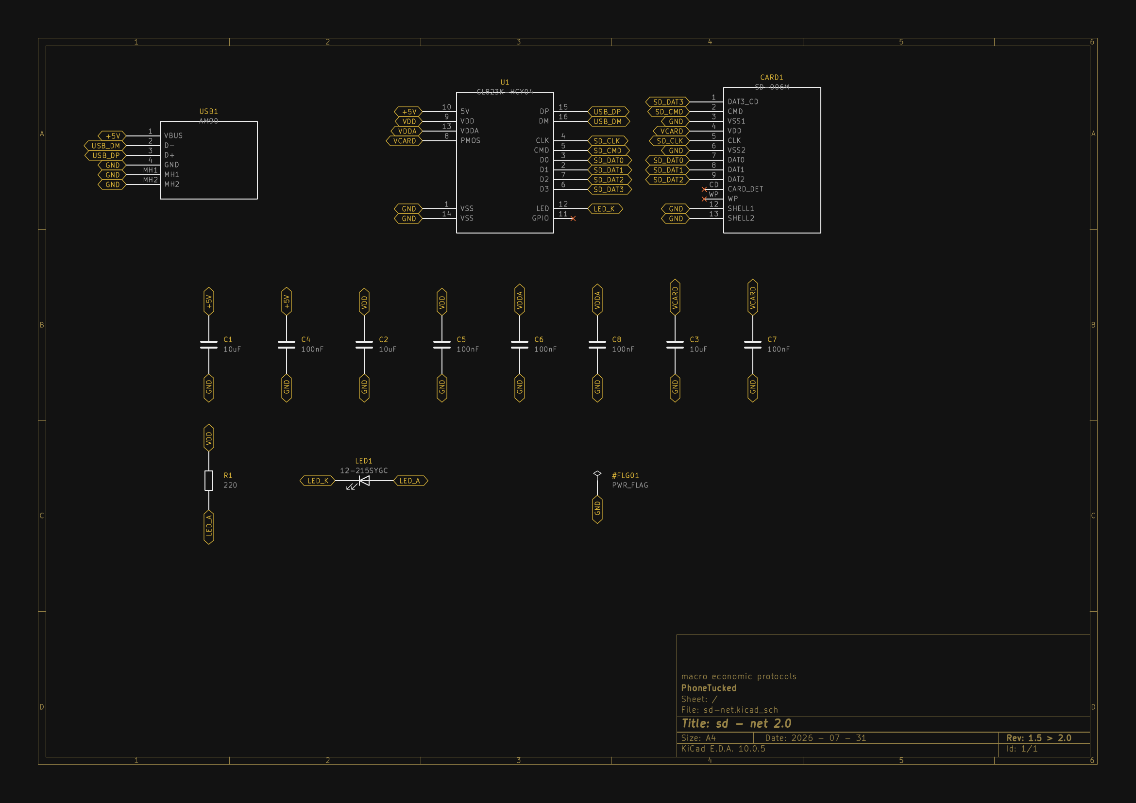
full-size USB SD card reader > USB-A plug for end user connect > 13 placements across 7 line items in between.

live: [github.com/1phonetucked-tech/sd-net-2.0](https://github.com/1phonetucked-tech/sd-net-2.0)
certificate: [OSHWA US002843](https://certification.oshwa.org/us002843.html)
sponsor: [PCBWay](https://www.pcbway.com/)

rev 2.0 is certified open source hardware by the Open Source Hardware Association > UID US002843 > certified 2026 - 08 - 07

hardware, everything in `hardware/` and `fab/` > CERN-OHL-S-2.0 > distribute a variant and its design files must be shared under the same terms
documentation, everything in `docs/` > CC-BY-SA-4.0 > credit the source, share adaptations alike
software, the generators in `tools/` > GPL-3.0 > see `tools/LICENSE`

| controller | Genesys Logic GL823K, SSOP-16, LCSC C284879 |
| board | 116.12 × 64.98 mm, 4 layers, 1.6 mm, ENIG |
| finish | black soldermask, white legend |
| placements | 13, of which 12 SMT and 1 through-hole |
| interface | USB 2.0 high speed, SD 4-bit mode |

boards are exclusively given away > not sold

**rev 2.0 is currently in production**

**shoutout to PCBWay who is sponsoring the rev 2.0 run > five boards, fabricated and assembled**

## specifications

**supply**
1 external rail. GL823K's only rated input is 5 V from VBUS (multimeter tested). VDD and VDDA are outputs of an on-chip band-gap regulator and carry decoupling only > never an external feed. card power is a separate switched net driven from the controller's current-limited output, with its bulk capacitance at the socket so card inrush never reaches the USB PHY rail. **four nets > eight capacitors > no external regulator**
review [`docs/POWER-DESIGN.md`](docs/POWER-DESIGN.md)

**land patterns**
KiCad ships no footprint matching any of the three parts on this board > SD-006M (SD slot) > AM90 (USB) > Everlight 12-215SYGC/S530-E2/TR8 (LED). i opted out of pulling them from easyeda2kicad and generated them from the manufacturers' recommended land patterns instead > dimension by dimension > 3D models the same way. every value is recorded in [`docs/LAND-PATTERNS.md`](docs/LAND-PATTERNS.md) > the USB plug's shell tabs sit in correctly sized plated slots rather than oversized round holes > those tabs are the only thing anchoring a board that cantilevers roughly 75 mm out of a host port

**outline**
isosceles triangle > symmetric about the axis the apex arc and all three connectors sit on > both sides 70.175 mm at 48.007 degrees, with the diagonals constructed as true tangents to the corner fillets

**no external clock**
controller (GL823K-HCY04) has an on-chip clock source > 12 MHz crystal is not required.

**no card detect**
by design. controller detects cards by polling the SD bus, which is why the socket's mechanical CD and WP are no connect

## currently

design is DRC clean.
0 violations and 0 unconnected
netlist is checked against intent > supply topology is confirmed on hardware at 3.38 V

created by (1)PhoneTucked